
$4.5 Million Secured by Skyhawk LTE Connected Monitoring Devices
PICA Product Development (PPD), an industry leading manufacturer of intelligent music-on-hold, in-store messaging and loss prevention systems and its affiliate company, PICA Manufacturing Solutions (PMS), a leading manufacturer of Flexible and Rigid Circuits, announced the securing of a $4.5 million line of credit from Bank of America to assist the market introduction of PPD's Skyhawk line of IoT remote monitoring devices.
Newly deployed LTE Cat M1 networks, providing coverage of essentially the entire United States, are now supporting Low Power Wide Area Network (LPWAN) technology. What this means for users is that the latest Internet of Things (IoT) monitoring devices can combine LTE mobile connectivity with extremely long battery life. The Skyhawk product line is specially engineered to take full advantage of these new technologies and allow very long-term deployment of monitoring devices for various use cases.
Highly compact Skyhawk devices feature potent internal primary battery power enabling rapid long-term deployment of various types of sensors to monitor assets in remote locations without the need for any other connectivity or power sources. Additionally, Skyhawk deployment and customer activation are entirely mobile device App based, eliminating the need for complicated manual setup processes. The Skyhawk hardware and connectivity services are provided with customized software solutions for various consumer, commercial and industrial applications. Custom integration into existing deployed enterprise business software via our API solutions is also supported.
Application areas will include animal relocation, wildlife control, pest management, tank monitoring, marine, environmental monitoring, graffiti prevention, perimeter security, delivery notification, remote building/storage monitoring, remote asset monitoring, construction site monitoring, equipment monitoring, automobile loT security, employee security and a host of other applications not previously practical or economical. Initial product introductions are being made at the 2019 Animal Care Expo – booth 914.
In addition to the new $4.5 million line of credit, the design, manufacturing and financial resources of the PICA group of companies will continue to the facilitate development and marketing of the Skyhawk product line.
ABOUT SKYHAWK
Skyhawk, a product line of PICA Product Development, are leading edge IoT remote monitoring devices which utilize LTE Cat M1 mobile telecommunications technology. All Skyhawk devices are engineered for ultra-long battery life creating a "best-in-class" product line designed to be deployed in locations which do not offer easily accessible power or Wi-Fi.
For more information about Skyhawk, please visit www.sky-hawk.com.
For more information about PICA Manufacturing Solutions, please visit www.picamfg.com.
Solder Paste Jetting for Flex PCB Assembly
Solder Paste Jetting Overcomes a lot of the Solder Deposition Issues with Today’s Flex Circuit Assembly
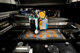
At PICA we do a lot of Flex Circuit Assembly (FCA) for our valued Customers. They ask us to install 0201 and 0.35mm pitch components on FCAs. Here are a few of the challenges with solder deposition on FCAs.
- Flex Circuits can have shrink and to a lesser degree stretch from lot to lot.
- Flex Circuits often have stiffeners that are above the plane of the components.
- Some FCAs with 0201 and 0.35mm pitch components will have other larger components and connectors that depend on significant deposits of solder for mechanical strength.
The amount of shrink associated with Flex Circuits becomes an issue when dealing with 0201 and 0.4mm and below pitch components. A solder paste stencil cannot shrink and stretch to match up with the Flex. Our MY600JX Solder Paste Jetter looks at features on the Flex such as fiducials or component pads and shrinks or stretches the program to match the circuit. This capability is essential when processing FCAs that have an area of 18mm square with 327 Opportunities for a Defect.
It is common for Flex Circuits to have stiffeners in locations that require a rigid support that are +Z to the plane of the circuit. If the stiffener is 0.5mm or less and components are not close to it, a solder paste stencil can work. With our Solder Paste Jetter, this becomes a non-issue. Z keep out areas are programmed in to insure the Print Head does not collide with the stiffener while still allowing very precise paste application near the stiffener.
The FCAs of today often have very small and very fine pitch components intermixed with larger components. With the solder paste stencil approach it can be a challenge when you have components requiring a very precise and minute amount of solder deposition to avoid bridging, next to components requiring larger depositions for mechanical strength. Step-up or step-down stencils can be a solution on some designs if there is sufficient clearance between the base stencil and the step-up or step-down. Most of today’s designs do not allow this option. With our Solder Paste Jetter we can jet a pad at a 0.002” stencil equivalent right next to a pad with 0.01” stencil equivalent.
Here is an example of a FCA that is using the capability of Jetting various deposition percentages to have the effect of different stencil thicknesses.
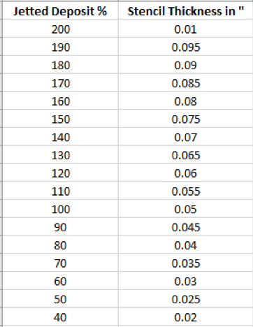
PICA is increasingly seeing FCA’s that the traditional solder paste stencil process is not an option. Solder Paste Jetting has proven to be a very viable and reliable solution.

The Art Of Team Building: POSITIVE ENERGY
As Director of PICA Manufacturing Asian Operations for over seven years, I’ve had the honor of leading our team to achieve the company’s objectives while staying true to the corporate strategy. So far we’ve exceeded our expectations, not only in terms of company revenue and profit, but also in employee engagement.
And what’s the number one lesson I’ve learned from the PICA Manufacturing success? No one can be successful without the help of teammates—it’s all about team building and team spirit.
People are the most valuable resources to small size companies. Ultimately, inside any organization, it’s people who make things happen and people who drive success. And the main factor that allows a team to work well together is a positive mindset, or as we call it in Chinese, Zheng Neng Liang (正能量). It’s an important rule of human interaction: one person with a positive attitude can motivate the rest of the team to invest in company performance.
This idea has led me to contemplate through all these years about how to magnify this “positive energy” and spread it among our company’s team members as well as to individuals external to the company. The answer is through team building!
Every company has their own definitions of team building. Mine is centered around basic human interactions, such as:
- Socializing and spending time together
- Looking after one another and helping each other out
- It’s never just ME, it’s WE
- Thinking of each other as a family
The goal is to make your team realize how powerful they can be if everyone channels this energy by helping each other out and aiming towards the same objective. I always remind my team members about the way wolves hunt a prey – it is through group strategy that the pack is able to take down the victim. Everyone knows their place and executes their specific role accordingly. This is pretty much what I want my team to understand about the concept of team building: forget about yourself (ego & selfishness) and understand that a great achievement comes from helping each other out. Ultimately this is what leads to team success —which is more meaningful than a person’s individual success!
During our annual off-site team building activities, the team usually plans a year in advance where the location will be and how it will align with the objectives set for that year. In the past 3 years we’ve been focusing on sites where the conditions are extreme, ranging from very cold to very hot climates. The team members really appreciate Pica’s commitment to these team building exercises and how it helps them excel in their respective functions.
Team Spirit runs deep in our hearts and will always play a large role in the management of my team.

Large Thermal Mass Component Hand Soldering
While mass soldering processes dominate soldering applications, hand soldering remains critical in the electronic manufacturing. Existing processes (e.g. convection oven reflow, vapor phase, wave flow, selective wave flow, etc.) are very efficient and offer high volume capacity but may not always be suitable.
One of these special situations is when the thermal mass of a few components to be soldered are relatively larger than the other components on the same substrate. In that case, we must consider a separate process for these components (i.e. separate reflow step or hand solder).
While hand soldering may appear to be simple, the same critical process elements exist as in mass soldering and must be controlled to achieve reliable solder joints. These include:
1. Heat source
- Reservoir soldering irons
- Constant tip temperature soldering irons
2. Heat transfer media
- Soldering iron tip. Size and configuration
3. Cleaning material (flux)
- Type. No Clean, RMA, OA, etc.
- Quantity
4. Time to achieve soldering
- Operator dependent
- Point of contact for solder and iron tip
Should it become necessary to use hand soldering due to large thermal mass issues, the following determinations and techniques need to be considered.
- Soldering iron selection. Large thermal mass components require a lot more energy transfer to achieve soldering temperatures. Heat reservoir type irons may not be capable of delivering this required amount or may have inadequate recovery time during repeated uses. These types of iron store the energy (heat) in a large thermal mass area and transfer it when the tip comes in contactwith the material to be soldered. Irons with constant tip temperature use a different technology to maintain the tip at a selected constant temperature regardless of the size of the component to be soldered.
- Tip selection. Tip selection is critical to effective heat transfer. Think of it as a gate which if inadequate will prevent efficient heat transfer or cause excessive thermal loss and tip deterioration. Tip configuration is determined by the size of the materials to be soldered. Maximize the contact area of the tip to the material; the greater the contact area the more efficient the heat transfer. Minimize tip non-contact areas as this promotes heat loss away from the joint. In contrast, too small a tip restricts heat transfer and increases soldering time which may result in unreliable solder connections.
- Cleaning Material Selection (Flux): Flux type is a trade-off between not having a post solder joint cleaning step or a more aggressive pre soldered components cleaning. While cleaning (oxide removal) is the primary function of the flux, facilitating heat transfer from the iron tip to the components is also critical. This involves having the proper amount of flux delivered to the connection. Core solder is common in hand soldering applications, which has the flux encapsulated in the center of the core. The amount of flux is determined by the size of the flux channel in the core solder and is a matter of choice. Too little flux will prevent proper heat transfer and proper cleaning.
- Time to Achieve Soldering. Allowing sufficient time for the components to come to proper temperature is perhaps the single most critical parameter in soldering. Mass soldering processes control this parameter by machine settings like the speed of the conveyor. Hand soldering however depends on the operator and is thus subject to a great degree of variability. For large mass components, more heat transfer is necessary to reach temperature (and thus more time). The best indicator is visual, such as when the solder melts – although this can be deceiving. The wrong way is when the soldering iron tip melts the solder first and then the melted solder deposits on the components. It causes improper intermetallic (non-wetting) and the bond between the solder and the components/PCB pads is compromised. It is important to understand that as the material to be soldered increases in mass, time to reach soldering temperature increases significantly and there is no means available to the operator to know when that occurs. Technique of soldering now becomes critical. Placing the solder iron tip directly on the components to be soldered and contacting the core solder to the same components surfaces (not the soldering iron tip) will permit the solder to be melted by the heat from the components rather than the soldering iron eliminating “Transfer Soldering”. Now, when the operator sees the solder melt, they know proper temperature of the solder surfaces has been reached.
The Thick & Thin of Flex
Consumer electronics and many commercial applications have demanded more be packed into thinner and lighter constructions; this puts a literal “squeeze” not only on the flexible circuits required but also the engineer who needs to satisfy the demand for thinner and thinner electronics. Adding layers is a good way to get more “action” within the same footprint but there are some considerations we must take into account if we want a reliable circuit.
We live by many design ‘rules’ but any engineer or PCB designer will admit to bending these rules on occasion. The key is to know how and when to bend these rules and the use of proper FMEA procedures to mitigate risk. I was thinking of these rules just the other day when I was reviewing a design for a very thick flex. Close attention to basic design rules becomes critical when we are asked to build a flex above six layers. At eight layers we need to pay close attention to every aspect of the design. Any application should be reviewed for basic electrical and mechanical requirements and a determination made as to the impact the material stack-up will have on both. Are we looking at a “formed” flex or is our circuit used in a dynamic application?
Let’s start with a quick review of what concerns us when we design a high layer-count flexible circuits, what potential failure modes are we likely to experience? Obviously as we add layers we add thickness. Each additional layer in turn requires an additional layer of adhesive. Our enemy here is Coefficient of Thermal Expansion (CTE), specifically the impact CTE has on our plated through holes. Though components with discrete leads requiring PTHs have become less common, there are still a large number of connectors and devices that require them (this is especially true in military applications). The more layers we add the more stresses we are placing on the PTH, or plated barrel during thermal excursions or thermal shock. In many cases it may not be as important to count the number of layers but to review the overall thickness and construction of the entire flex. This is where our “rules” may let us down.
IPC guidelines call for a minimum of 25um of copper plating on flex of 6 layers or less while requiring 35um on boards greater than 6 layers. This is regardless of actual board thickness. To be fair, these are indeed guidelines, no specification could possibly account for every possible variation within a circuit type. Regardless of the recommendations it is important for us as engineers and designers to review the stack-up carefully, examine the operating environment of the flexible circuits, and determine what we believe to be the best course to take. Remember these guidelines are minimums; it is up to us to determine if we require more for our particular application.
Summary:
Building higher count multi-layers requires careful consideration beyond “general” guidelines. The IPC design rules are a great place to start, but when you “push the envelope” you need to find a flex provider that can assist you in reviewing not only the design for manufacture, but can also offer a true application review.